source : wikipedia.org
A central processing unit (CPU), or sometimes just processor, is a description of a class of logic machines that can execute computer programs. This broad definition can easily be applied to many early computers that existed long before the term "CPU" ever came into widespread usage. However, the term itself and its initialism have been in use in the computer industry at least since the early 1960s (Weik 1961). The form, design and implementation of CPUs have changed dramatically since the earliest examples, but their fundamental operation has remained much the same.
Early CPUs were custom-designed as a part of a larger, usually one-of-a-kind, computer. However, this costly method of designing custom CPUs for a particular application has largely given way to the development of mass-produced processors that are suited for one or many purposes. This standardization trend generally began in the era of discrete transistor mainframes and minicomputers and has rapidly accelerated with the popularization of the integrated circuit (IC). The IC has allowed increasingly complex CPUs to be designed and manufactured in very small spaces (on the order of millimeters). Both the miniaturization and standardization of CPUs have increased the presence of these digital devices in modern life far beyond the limited application of dedicated computing machines. Modern microprocessors appear in everything from automobiles to cell phones to children's toys.
History of CPUs
-

EDVAC, one of the first electronic stored program computers.
Prior to the advent of machines that resemble today's CPUs, computers such as the ENIAC had to be physically rewired in order to perform different tasks. These machines are often referred to as "fixed-program computers," since they had to be physically reconfigured in order to run a different program. Since the term "CPU" is generally defined as a software (computer program) execution device, the earliest devices that could rightly be called CPUs came with the advent of the stored-program computer.
The idea of a stored-program computer was already present during ENIAC's design, but was initially omitted so the machine could be finished sooner. On June 30, 1945, before ENIAC was even completed, mathematician John von Neumann distributed the paper entitled "First Draft of a Report on the EDVAC." It outlined the design of a stored-program computer that would eventually be completed in August 1949 (von Neumann 1945). EDVAC was designed to perform a certain number of instructions (or operations) of various types. These instructions could be combined to create useful programs for the EDVAC to run. Significantly, the programs written for EDVAC were stored in high-speed computer memory rather than specified by the physical wiring of the computer. This overcame a severe limitation of ENIAC, which was the large amount of time and effort it took to reconfigure the computer to perform a new task. With von Neumann's design, the program, or software, that EDVAC ran could be changed simply by changing the contents of the computer's memory.[1]
While von Neumann is most often credited with the design of the stored-program computer because of his design of EDVAC, others before him such as Konrad Zuse had suggested similar ideas. Additionally, the so-called Harvard architecture of the Harvard Mark I, which was completed before EDVAC, also utilized a stored-program design using punched paper tape rather than electronic memory. The key difference between the von Neumann and Harvard architectures is that the latter separates the storage and treatment of CPU instructions and data, while the former uses the same memory space for both. Most modern CPUs are primarily von Neumann in design, but elements of the Harvard architecture are commonly seen as well.
Being digital devices, all CPUs deal with discrete states and therefore require some kind of switching elements to differentiate between and change these states. Prior to commercial acceptance of the transistor, electrical relays and vacuum tubes (thermionic valves) were commonly used as switching elements. Although these had distinct speed advantages over earlier, purely mechanical designs, they were unreliable for various reasons. For example, building direct current sequential logic circuits out of relays requires additional hardware to cope with the problem of contact bounce. While vacuum tubes do not suffer from contact bounce, they must heat up before becoming fully operational and eventually stop functioning altogether.[2] Usually, when a tube failed, the CPU would have to be diagnosed to locate the failing component so it could be replaced. Therefore, early electronic (vacuum tube based) computers were generally faster but less reliable than electromechanical (relay based) computers. Tube computers like EDVAC tended to average eight hours between failures, whereas relay computers like the (slower, but earlier) Harvard Mark I failed very rarely (Weik 1961:238). In the end, tube based CPUs became dominant because the significant speed advantages afforded generally outweighed the reliability problems. Most of these early synchronous CPUs ran at low clock rates compared to modern microelectronic designs (see below for a discussion of clock rate). Clock signal frequencies ranging from 100 kHz to 4 MHz were very common at this time, limited largely by the speed of the switching devices they were built with.
[edit] Discrete transistor and IC CPUs

A 4-bit, 2 register, six assembly language instruction computer made entirely of
74-series chips.
The design complexity of CPUs increased as various technologies facilitated building smaller and more reliable electronic devices. The first such improvement came with the advent of the transistor. Transistorized CPUs during the 1950s and 1960s no longer had to be built out of bulky, unreliable, and fragile switching elements like vacuum tubes and electrical relays. With this improvement more complex and reliable CPUs were built onto one or several printed circuit boards containing discrete (individual) components.
During this period, a method of manufacturing many transistors in a compact space gained popularity.The integrated circuit (IC) allowed a large number of transistors to be manufactured on a single semiconductor-based die, or "chip." At first only very basic non-specialized digital circuits such as NOR gates were miniaturized into ICs. CPUs based upon these "building block" ICs are generally referred to as "small-scale integration" (SSI) devices. SSI ICs, such as the ones used in the Apollo guidance computer, usually contained transistor counts numbering in multiples of ten. To build an entire CPU out of SSI ICs required thousands of individual chips, but still consumed much less space and power than earlier discrete transistor designs. As microelectronic technology advanced, an increasing number of transistors were placed on ICs, thus decreasing the quantity of individual ICs needed for a complete CPU. MSI and LSI (medium- and large-scale integration) ICs increased transistor counts to hundreds, then thousands.
In 1964 IBM introduced its System/360 computer architecture, which was used in a series of computers that could run the same programs with different speed and performance. This was significant at a time when most electronic computers were incompatible with one another, even those made by the same manufacturer. To facilitate this improvement, IBM utilized the concept of a microprogram (often called "microcode"), which still sees widespread usage in modern CPUs (Amdahl et al. 1964). The System/360 architecture was so popular that it dominated the mainframe computer market for the next few decades and left a legacy that is still continued by similar modern computers like the IBM zSeries. In the same year (1964), Digital Equipment Corporation (DEC) introduced another influential computer aimed at the scientific and research markets, the PDP-8. DEC would later introduce the extremely popular PDP-11 line that originally was built with SSI ICs but was eventually implemented with LSI components once these became practical. In stark contrast with its SSI and MSI predecessors, the first LSI implementation of the PDP-11 contained a CPU composed of only four LSI integrated circuits (Digital Equipment Corporation 1975).
Transistor-based computers had several distinct advantages over their predecessors. Aside from facilitating increased reliability and lower power consumption, transistors also allowed CPUs to operate at much higher speeds because of the short switching time of a transistor in comparison to a tube or relay. Thanks to both the increased reliability as well as the dramatically increased speed of the switching elements (which were almost exclusively transistors by this time), CPU clock rates in the tens of megahertz were obtained during this period. Additionally, while discrete transistor and IC CPUs were in heavy usage, new high-performance designs like SIMD (Single Instruction Multiple Data) vector processors began to appear. These early experimental designs later gave rise to the era of specialized supercomputers like those made by Cray Inc.
[edit] Microprocessors
-
Main article: Microprocessor
The introduction of the microprocessor in the 1970s significantly affected the design and implementation of CPUs. Since the introduction of the first microprocessor (the Intel 4004) in 1970 and the first widely used microprocessor (the Intel 8080) in 1974, this class of CPUs has almost completely overtaken all other central processing unit implementation methods. Mainframe and minicomputer manufacturers of the time launched proprietary IC development programs to upgrade their older computer architectures, and eventually produced instruction set compatible microprocessors that were backward-compatible with their older hardware and software. Combined with the advent and eventual vast success of the now ubiquitous personal computer, the term "CPU" is now applied almost exclusively to microprocessors.
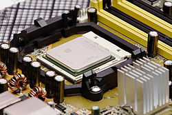
Previous generations of CPUs were implemented as discrete components and numerous small integrated circuits (ICs) on one or more circuit boards. Microprocessors, on the other hand, are CPUs manufactured on a very small number of ICs; usually just one. The overall smaller CPU size as a result of being implemented on a single die means faster switching time because of physical factors like decreased gate parasitic capacitance. This has allowed synchronous microprocessors to have clock rates ranging from tens of megahertz to several gigahertz. Additionally, as the ability to construct exceedingly small transistors on an IC has increased, the complexity and number of transistors in a single CPU has increased dramatically. This widely observed trend is described by Moore's law, which has proven to be a fairly accurate predictor of the growth of CPU (and other IC) complexity to date.
While the complexity, size, construction, and general form of CPUs have changed drastically over the past sixty years, it is notable that the basic design and function has not changed much at all. Almost all common CPUs today can be very accurately described as von Neumann stored-program machines. As the aforementioned Moore's law continues to hold true, concerns have arisen about the limits of integrated circuit transistor technology. Extreme miniaturization of electronic gates is causing the effects of phenomena like electromigration and subthreshold leakage to become much more significant. These newer concerns are among the many factors causing researchers to investigate new methods of computing such as the quantum computer, as well as to expand the usage of parallelism and other methods that extend the usefulness of the classical von Neumann model.
[edit] CPU operation
The fundamental operation of most CPUs, regardless of the physical form they take, is to execute a sequence of stored instructions called a program. Discussed here are devices that conform to the common von Neumann architecture. The program is represented by a series of numbers that are kept in some kind of computer memory. There are four steps that nearly all von Neumann CPUs use in their operation: fetch, decode, execute, and writeback.
The first step, fetch, involves retrieving an instruction (which is represented by a number or sequence of numbers) from program memory. The location in program memory is determined by a program counter (PC), which stores a number that identifies the current position in the program. In other words, the program counter keeps track of the CPU's place in the current program. After an instruction is fetched, the PC is incremented by the length of the instruction word in terms of memory units.[3] Often the instruction to be fetched must be retrieved from relatively slow memory, causing the CPU to stall while waiting for the instruction to be returned. This issue is largely addressed in modern processors by caches and pipeline architectures (see below).
The instruction that the CPU fetches from memory is used to determine what the CPU is to do. In the decode step, the instruction is broken up into parts that have significance to other portions of the CPU. The way in which the numerical instruction value is interpreted is defined by the CPU's instruction set architecture (ISA).[4] Often, one group of numbers in the instruction, called the opcode, indicates which operation to perform. The remaining parts of the number usually provide information required for that instruction, such as operands for an addition operation. Such operands may be given as a constant value (called an immediate value), or as a place to locate a value: a register or a memory address, as determined by some addressing mode. In older designs the portions of the CPU responsible for instruction decoding were unchangeable hardware devices. However, in more abstract and complicated CPUs and ISAs, a microprogram is often used to assist in translating instructions into various configuration signals for the CPU. This microprogram is sometimes rewritable so that it can be modified to change the way the CPU decodes instructions even after it has been manufactured.

Block diagram of a simple CPU
After the fetch and decode steps, the execute step is performed. During this step, various portions of the CPU are connected so they can perform the desired operation. If, for instance, an addition operation was requested, an arithmetic logic unit (ALU) will be connected to a set of inputs and a set of outputs. The inputs provide the numbers to be added, and the outputs will contain the final sum. The ALU contains the circuitry to perform simple arithmetic and logical operations on the inputs (like addition and bitwise operations). If the addition operation produces a result too large for the CPU to handle, an arithmetic overflow flag in a flags register may also be set (see the discussion of integer range below).
The final step, writeback, simply "writes back" the results of the execute step to some form of memory. Very often the results are written to some internal CPU register for quick access by subsequent instructions. In other cases results may be written to slower, but cheaper and larger, main memory. Some types of instructions manipulate the program counter rather than directly produce result data. These are generally called "jumps" and facilitate behavior like loops, conditional program execution (through the use of a conditional jump), and functions in programs.[5] Many instructions will also change the state of digits in a "flags" register. These flags can be used to influence how a program behaves, since they often indicate the outcome of various operations. For example, one type of "compare" instruction considers two values and sets a number in the flags register according to which one is greater. This flag could then be used by a later jump instruction to determine program flow.
After the execution of the instruction and writeback of the resulting data, the entire process repeats, with the next instruction cycle normally fetching the next-in-sequence instruction because of the incremented value in the program counter. If the completed instruction was a jump, the program counter will be modified to contain the address of the instruction that was jumped to, and program execution continues normally. In more complex CPUs than the one described here, multiple instructions can be fetched, decoded, and executed simultaneously. This section describes what is generally referred to as the "Classic RISC pipeline," which in fact is quite common among the simple CPUs used in many electronic devices (often called microcontrollers[clarify]).[6]
[edit] Design and implementation
-
[edit] Integer range
The way a CPU represents numbers is a design choice that affects the most basic ways in which the device functions. Some early digital computers used an electrical model of the common decimal (base ten) numeral system to represent numbers internally. A few other computers have used more exotic numeral systems like ternary (base three). Nearly all modern CPUs represent numbers in binary form, with each digit being represented by some two-valued physical quantity such as a "high" or "low" voltage.[7]
Related to number representation is the size and precision of numbers that a CPU can represent. In the case of a binary CPU, a bit refers to one significant place in the numbers a CPU deals with. The number of bits (or numeral places) a CPU uses to represent numbers is often called "word size", "bit width", "data path width", or "integer precision" when dealing with strictly integer numbers (as opposed to floating point). This number differs between architectures, and often within different parts of the very same CPU. For example, an 8-bit CPU deals with a range of numbers that can be represented by eight binary digits (each digit having two possible values), that is, 28 or 256 discrete numbers. In effect, integer size sets a hardware limit on the range of integers the software run by the CPU can utilize.[8]
Integer range can also affect the number of locations in memory the CPU can address (locate). For example, if a binary CPU uses 32 bits to represent a memory address, and each memory address represents one octet (8 bits), the maximum quantity of memory that CPU can address is 232 octets, or 4 GiB. This is a very simple view of CPU address space, and many designs use more complex addressing methods like paging in order to locate more memory than their integer range would allow with a flat address space.
Higher levels of integer range require more structures to deal with the additional digits, and therefore more complexity, size, power usage, and general expense. It is not at all uncommon, therefore, to see 4- or 8-bit microcontrollers used in modern applications, even though CPUs with much higher range (such as 16, 32, 64, even 128-bit) are available. The simpler microcontrollers are usually cheaper, use less power, and therefore dissipate less heat, all of which can be major design considerations for electronic devices. However, in higher-end applications, the benefits afforded by the extra range (most often the additional address space) are more significant and often affect design choices. To gain some of the advantages afforded by both lower and higher bit lengths, many CPUs are designed with different bit widths for different portions of the device. For example, the IBM System/370 used a CPU that was primarily 32 bit, but it used 128-bit precision inside its floating point units to facilitate greater accuracy and range in floating point numbers (Amdahl et al. 1964). Many later CPU designs use similar mixed bit width, especially when the processor is meant for general-purpose usage where a reasonable balance of integer and floating point capability is required.
[edit] Clock rate
-
Most CPUs, and indeed most sequential logic devices, are synchronous in nature.[9] That is, they are designed and operate on assumptions about a synchronization signal. This signal, known as a clock signal, usually takes the form of a periodic square wave. By calculating the maximum time that electrical signals can move in various branches of a CPU's many circuits, the designers can select an appropriate period for the clock signal.
This period must be longer than the amount of time it takes for a signal to move, or propagate, in the worst-case scenario. In setting the clock period to a value well above the worst-case propagation delay, it is possible to design the entire CPU and the way it moves data around the "edges" of the rising and falling clock signal. This has the advantage of simplifying the CPU significantly, both from a design perspective and a component-count perspective. However, it also carries the disadvantage that the entire CPU must wait on its slowest elements, even though some portions of it are much faster. This limitation has largely been compensated for by various methods of increasing CPU parallelism (see below).
However architectural improvements alone do not solve all of the drawbacks of globally synchronous CPUs. For example, a clock signal is subject to the delays of any other electrical signal. Higher clock rates in increasingly complex CPUs make it more difficult to keep the clock signal in phase (synchronized) throughout the entire unit. This has led many modern CPUs to require multiple identical clock signals to be provided in order to avoid delaying a single signal significantly enough to cause the CPU to malfunction. Another major issue as clock rates increase dramatically is the amount of heat that is dissipated by the CPU. The constantly changing clock causes many components to switch regardless of whether they are being used at that time. In general, a component that is switching uses more energy than an element in a static state. Therefore, as clock rate increases, so does heat dissipation, causing the CPU to require more effective cooling solutions.
One method of dealing with the switching of unneeded components is called clock gating, which involves turning off the clock signal to unneeded components (effectively disabling them). However, this is often regarded as difficult to implement and therefore does not see common usage outside of very low-power designs.[10] Another method of addressing some of the problems with a global clock signal is the removal of the clock signal altogether. While removing the global clock signal makes the design process considerably more complex in many ways, asynchronous (or clockless) designs carry marked advantages in power consumption and heat dissipation in comparison with similar synchronous designs. While somewhat uncommon, entire CPUs have been built without utilizing a global clock signal. Two notable examples of this are the ARM compliant AMULET and the MIPS R3000 compatible MiniMIPS. Rather than totally removing the clock signal, some CPU designs allow certain portions of the device to be asynchronous, such as using asynchronous ALUs in conjunction with superscalar pipelining to achieve some arithmetic performance gains. While it is not altogether clear whether totally asynchronous designs can perform at a comparable or better level than their synchronous counterparts, it is evident that they do at least excel in simpler math operations. This, combined with their excellent power consumption and heat dissipation properties, makes them very suitable for embedded computers (Garside et al. 1999).
[edit] Parallelism
-

Model of a subscalar CPU. Notice that it takes fifteen cycles to complete three instructions.
The description of the basic operation of a CPU offered in the previous section describes the simplest form that a CPU can take. This type of CPU, usually referred to as subscalar, operates on and executes one instruction on one or two pieces of data at a time.
This process gives rise to an inherent inefficiency in subscalar CPUs. Since only one instruction is executed at a time, the entire CPU must wait for that instruction to complete before proceeding to the next instruction. As a result the subscalar CPU gets "hung up" on instructions which take more than one clock cycle to complete execution. Even adding a second execution unit (see below) does not improve performance much; rather than one pathway being hung up, now two pathways are hung up and the number of unused transistors is increased. This design, wherein the CPU's execution resources can operate on only one instruction at a time, can only possibly reach scalar performance (one instruction per clock). However, the performance is nearly always subscalar (less than one instruction per cycle).
Attempts to achieve scalar and better performance have resulted in a variety of design methodologies that cause the CPU to behave less linearly and more in parallel. When referring to parallelism in CPUs, two terms are generally used to classify these design techniques. Instruction level parallelism (ILP) seeks to increase the rate at which instructions are executed within a CPU (that is, to increase the utilization of on-die execution resources), and thread level parallelism (TLP) purposes to increase the number of threads (effectively individual programs) that a CPU can execute simultaneously. Each methodology differs both in the ways in which they are implemented, as well as the relative effectiveness they afford in increasing the CPU's performance for an application.[11]
[edit] Instruction level parallelism
-

Basic five-stage pipeline. In the best case scenario, this pipeline can sustain a completion rate of one instruction per cycle.
One of the simplest methods used to accomplish increased parallelism is to begin the first steps of instruction fetching and decoding before the prior instruction finishes executing. This is the simplest form of a technique known as instruction pipelining, and is utilized in almost all modern general-purpose CPUs. Pipelining allows more than one instruction to be executed at any given time by breaking down the execution pathway into discrete stages. This separation can be compared to an assembly line, in which an instruction is made more complete at each stage until it exits the execution pipeline and is retired.
Pipelining does, however, introduce the possibility for a situation where the result of the previous operation is needed to complete the next operation; a condition often termed data dependency conflict. To cope with this, additional care must be taken to check for these sorts of conditions and delay a portion of the instruction pipeline if this occurs. Naturally, accomplishing this requires additional circuitry, so pipelined processors are more complex than subscalar ones (though not very significantly so). A pipelined processor can become very nearly scalar, inhibited only by pipeline stalls (an instruction spending more than one clock cycle in a stage).

Simple superscalar pipeline. By fetching and dispatching two instructions at a time, a maximum of two instructions per cycle can be completed.
Further improvement upon the idea of instruction pipelining led to the development of a method that decreases the idle time of CPU components even further. Designs that are said to be superscalar include a long instruction pipeline and multiple identical execution units. [Huynh 2003] In a superscalar pipeline, multiple instructions are read and passed to a dispatcher, which decides whether or not the instructions can be executed in parallel (simultaneously). If so they are dispatched to available execution units, resulting in the ability for several instructions to be executed simultaneously. In general, the more instructions a superscalar CPU is able to dispatch simultaneously to waiting execution units, the more instructions will be completed in a given cycle.
Most of the difficulty in the design of a superscalar CPU architecture lies in creating an effective dispatcher. The dispatcher needs to be able to quickly and correctly determine whether instructions can be executed in parallel, as well as dispatch them in such a way as to keep as many execution units busy as possible. This requires that the instruction pipeline is filled as often as possible and gives rise to the need in superscalar architectures for significant amounts of CPU cache. It also makes hazard-avoiding techniques like branch prediction, speculative execution, and out-of-order execution crucial to maintaining high levels of performance. By attempting to predict which branch (or path) a conditional instruction will take, the CPU can minimize the number of times that the entire pipeline must wait until a conditional instruction is completed. Speculative execution often provides modest performance increases by executing portions of code that may or may not be needed after a conditional operation completes. Out-of-order execution somewhat rearranges the order in which instructions are executed to reduce delays due to data dependencies.
In the case where a portion of the CPU is superscalar and part is not, the part which is not suffers a performance penalty due to scheduling stalls. The original Intel Pentium (P5) had two superscalar ALUs which could accept one instruction per clock each, but its FPU could not accept one instruction per clock. Thus the P5 was integer superscalar but not floating point superscalar. Intel's successor to the Pentium architecture, P6, added superscalar capabilities to its floating point features, and therefore afforded a significant increase in floating point instruction performance.
Both simple pipelining and superscalar design increase a CPU's ILP by allowing a single processor to complete execution of instructions at rates surpassing one instruction per cycle (IPC).[12] Most modern CPU designs are at least somewhat superscalar, and nearly all general purpose CPUs designed in the last decade are superscalar. In later years some of the emphasis in designing high-ILP computers has been moved out of the CPU's hardware and into its software interface, or ISA. The strategy of the very long instruction word (VLIW) causes some ILP to become implied directly by the software, reducing the amount of work the CPU must perform to boost ILP and thereby reducing the design's complexity.
[edit] Thread level parallelism
Another strategy of achieving performance is to execute multiple programs or threads in parallel. This area of research is known as parallel computing. In Flynn's taxonomy, this strategy is known as Multiple Instructions-Multiple Data or MIMD.
One technology used for this purpose was multiprocessing (MP). The initial flavor of this technology is known as symmetric multiprocessing (SMP), where a small number of CPUs share a coherent view of their memory system. In this scheme, each CPU has additional hardware to maintain a constantly up-to-date view of memory. By avoiding stale views of memory, the CPUs can cooperate on the same program and programs can migrate from one CPU to another. To increase the number of cooperating CPUs beyond a handful, schemes such as non-uniform memory access (NUMA) and directory-based coherence protocols were introduced in the 1990s. SMP systems are limited to a small number of CPUs while NUMA systems have been built with thousands of processors. Initially, multiprocessing was built using multiple discrete CPUs and boards to implement the interconnect between the processors. When the processors and their interconnect are all implemented on a single silicon chip, the technology is known as a multi-core microprocessor.
It was later recognized that finer-grain parallelism existed with a single program. A single program might have several threads (or functions) that could be executed separately or in parallel. Some of earliest examples of this technology implemented input/output processing such as direct memory access as a separate thread from the computation thread. A more general approach to this technology was introduced in the 1970s when systems were designed to run multiple computation threads in parallel. This technology is known as multi-threading (MT). This approach is considered more cost-effective than multiprocessing, as only a small number of components within a CPU is replicated in order to support MT as opposed to the entire CPU in the case of MP. In MT, the execution units and the memory system including the caches are shared among multiple threads. The downside of MT is that the hardware support for multithreading is more visible to software than that of MP and thus supervisor software like operating systems have to undergo larger changes to support MT. One type of MT that was implemented is known as block multithreading, where one thread is executed until it is stalled waiting for data to return from external memory. In this scheme, the CPU would then quickly switch to another thread which is ready to run, the switch often done in one CPU clock cycle. Another type of MT is known as simultaneous multithreading, where instructions of multiple threads are executed in parallel within one CPU clock cycle.
For several decades from the 1970s to early 2000s, the focus in designing high performance general purpose CPUs was largely on achieving high ILP through technologies such as pipelining, caches, superscalar execution, Out-of-order execution, etc. This trend culminated in large, power-hungry CPUs such as the Intel Pentium 4. By the early 2000s, CPU designers were thwarted from achieving higher performance from ILP techniques due to the growing disparity between CPU operating frequencies and main memory operating frequencies as well as escalating CPU power dissipation owing to more esoteric ILP techniques.
CPU designers then borrowed ideas from commercial computing markets such as transaction processing, where the aggregate performance of multiple programs, also known as throughput computing, was more important than the performance of a single thread or program.
This reversal of emphasis is evidenced by the proliferation of dual and multiple core CMP (chip-level multiprocessing) designs and notably, Intel's newer designs resembling its less superscalar P6 architecture. Late designs in several processor families exhibit CMP, including the x86-64 Opteron and Athlon 64 X2, the SPARC UltraSPARC T1, IBM POWER4 and POWER5, as well as several video game console CPUs like the Xbox 360's triple-core PowerPC design.
[edit] Data parallelism
-
Main articles: Vector processor and SIMD
A less common but increasingly important paradigm of CPUs (and indeed, computing in general) deals with data parallelism. The processors discussed earlier are all referred to as some type of scalar device.[13] As the name implies, vector processors deal with multiple pieces of data in the context of one instruction. This contrasts with scalar processors, which deal with one piece of data for every instruction. Using Flynn's taxonomy, these two schemes of dealing with data are generally referred to as SISD (single instruction, single data) and SIMD (single instruction, multiple data), respectively. The great utility in creating CPUs that deal with vectors of data lies in optimizing tasks that tend to require the same operation (for example, a sum or a dot product) to be performed on a large set of data. Some classic examples of these types of tasks are multimedia applications (images, video, and sound), as well as many types of scientific and engineering tasks. Whereas a scalar CPU must complete the entire process of fetching, decoding, and executing each instruction and value in a set of data, a vector CPU can perform a single operation on a comparatively large set of data with one instruction. Of course, this is only possible when the application tends to require many steps which apply one operation to a large set of data.
Most early vector CPUs, such as the Cray-1, were associated almost exclusively with scientific research and cryptography applications. However, as multimedia has largely shifted to digital media, the need for some form of SIMD in general-purpose CPUs has become significant. Shortly after floating point execution units started to become commonplace to include in general-purpose processors, specifications for and implementations of SIMD execution units also began to appear for general-purpose CPUs. Some of these early SIMD specifications like Intel's MMX were integer-only. This proved to be a significant impediment for some software developers, since many of the applications that benefit from SIMD primarily deal with floating point numbers. Progressively, these early designs were refined and remade into some of the common, modern SIMD specifications, which are usually associated with one ISA. Some notable modern examples are Intel's SSE and the PowerPC-related AltiVec (also known as VMX).[14]
Microprocessor
History
-
[edit] First types

The 4004 with cover removed (left) and as actually used (right).
Three projects arguably delivered a complete microprocessor at about the same time, namely Intel's 4004, the Texas Instruments (TI) TMS 1000, and Garrett AiResearch's Central Air Data Computer (CADC).
In 1968, Garrett AiResearch, with designer Ray Holt and Steve Geller, were invited to produce a digital computer to compete with electromechanical systems then under development for the main flight control computer in the US Navy's new F-14 Tomcat fighter. The design was complete by 1970, and used a MOS-based chipset as the core CPU. The design was significantly (approximately 20 times) smaller and much more reliable than the mechanical systems it competed against, and was used in all of the early Tomcat models. This system contained a "a 20-bit, pipelined, parallel multi-microprocessor". However, the system was considered so advanced that the Navy refused to allow publication of the design until 1997. For this reason the CADC, and the MP944 chipset it used, are fairly unknown even today. (see First Microprocessor Chip Set.) TI developed the 4-bit TMS 1000, and stressed pre-programmed embedded applications, introducing a version called the TMS1802NC on September 17, 1971, which implemented a calculator on a chip. The Intel chip was the 4-bit 4004, released on November 15, 1971, developed by Federico Faggin and Marcian Hoff, the manager of the designing team was Leslie L. Vadász.
TI filed for the patent on the microprocessor. Gary Boone was awarded U.S. Patent 3,757,306 for the single-chip microprocessor architecture on September 4, 1973. It may never be known which company actually had the first working microprocessor running on the lab bench. In both 1971 and 1976, Intel and TI entered into broad patent cross-licensing agreements, with Intel paying royalties to TI for the microprocessor patent. A nice history of these events is contained in court documentation from a legal dispute between Cyrix and Intel, with TI as intervenor and owner of the microprocessor patent.
Interestingly, a third party (Gilbert Hyatt) was awarded a patent which might cover the "microprocessor". See a webpage claiming an invention pre-dating both TI and Intel, describing a "microcontroller". According to a rebuttal and a commentary, the patent was later invalidated, but not before substantial royalties were paid out.
A computer-on-a-chip is a variation of a microprocessor which combines the microprocessor core (CPU), some memory, and I/O (input/output) lines, all on one chip. The computer-on-a-chip patent, called the "microcomputer patent" at the time, U.S. Patent 4,074,351 , was awarded to Gary Boone and Michael J. Cochran of TI. Aside from this patent, the standard meaning of microcomputer is a computer using one or more microprocessors as its CPU(s), while the concept defined in the patent is perhaps more akin to a microcontroller.
According to A History of Modern Computing, (MIT Press), pp. 220–21, Intel entered into a contract with Computer Terminals Corporation, later called Datapoint, of San Antonio TX, for a chip for a terminal they were designing. Datapoint later decided to use the chip, and Intel marketed it as the 8008 in April, 1972. This was the world's first 8-bit microprocessor. It was the basis for the famous "Mark-8" computer kit advertised in the magazine Radio-Electronics in 1974. The 8008 and its successor, the world-famous 8080, opened up the microprocessor component marketplace.
[edit] Notable 8-bit designs
The 4004 was later followed in 1972 by the 8008, the world's first 8-bit microprocessor. These processors are the precursors to the very successful Intel 8080 (1974), Zilog Z80 (1976), and derivative Intel 8-bit processors. The competing Motorola 6800 was released August 1974. Its architecture was cloned and improved in the MOS Technology 6502 in 1975, rivaling the Z80 in popularity during the 1980s.
Both the Z80 and 6502 concentrated on low overall cost, through a combination of small packaging, simple computer bus requirements, and the inclusion of circuitry that would normally have to be provided in a separate chip (for instance, the Z80 included a memory controller). It was these features that allowed the home computer "revolution" to take off in the early 1980s, eventually delivering such inexpensive machines as the Sinclair ZX-81, which sold for US$99.
The Western Design Center, Inc. (WDC) introduced the CMOS 65C02 in 1982 and licensed the design to several companies which became the core of the Apple IIc and IIe personal computers, medical implantable grade pacemakers and defibrilators, automotive, industrial and consumer devices.WDC pioneered the licensing of microprocessor technology which was later followed by ARM and other microprocessor Intellectual Property (IP) providers in the 1990’s.
Motorola trumped the entire 8-bit world by introducing the MC6809 in 1978, arguably one of the most powerful, orthogonal, and clean 8-bit microprocessor designs ever fielded – and also one of the most complex hard-wired logic designs that ever made it into production for any microprocessor. Microcoding replaced hardwired logic at about this point in time for all designs more powerful than the MC6809 – specifically because the design requirements were getting too complex for hardwired logic.
Another early 8-bit microprocessor was the Signetics 2650, which enjoyed a brief flurry of interest due to its innovative and powerful instruction set architecture.
A seminal microprocessor in the world of spaceflight was RCA's RCA 1802 (aka CDP1802, RCA COSMAC) (introduced in 1976) which was used in NASA's Voyager and Viking spaceprobes of the 1970s, and onboard the Galileo probe to Jupiter (launched 1989, arrived 1995). RCA COSMAC was the first to implement C-MOS technology. The CDP1802 was used because it could be run at very low power, and because its production process (Silicon on Sapphire) ensured much better protection against cosmic radiation and electrostatic discharges than that of any other processor of the era. Thus, the 1802 is said to be the first radiation-hardened microprocessor.
The RCA 1802 had what is called a static design, meaning that the clock frequency could be made arbitrarily low, even to 0 Hz, a total stop condition. This let the Voyager/Viking/Galileo spacecraft use minimum electric power for long uneventful stretches of a voyage. Timers and/or sensors would awaken/speed up the processor in time for important tasks, such as navigation updates, attitude control, data acquisition, and radio communication.
[edit] 16-bit designs
The first multi-chip 16-bit microprocessor was the National Semiconductor IMP-16, introduced in early 1973. An 8-bit version of the chipset was introduced in 1974 as the IMP-8. During the same year, National introduced the first 16-bit single-chip microprocessor, the National Semiconductor PACE, which was later followed by an NMOS version, the INS8900.
Other early multi-chip 16-bit microprocessors include one used by Digital Equipment Corporation (DEC) in the LSI-11 OEM board set and the packaged PDP 11/03 minicomputer, and the Fairchild Semiconductor MicroFlame 9440, both of which were introduced in the 1975 to 1976 timeframe.
The first single-chip 16-bit microprocessor was TI's TMS 9900, which was also compatible with their TI-990 line of minicomputers. The 9900 was used in the TI 990/4 minicomputer, the TI-99/4A home computer, and the TM990 line of OEM microcomputer boards. The chip was packaged in a large ceramic 64-pin DIP package, while most 8-bit microprocessors such as the Intel 8080 used the more common, smaller, and less expensive plastic 40-pin DIP. A follow-on chip, the TMS 9980, was designed to compete with the Intel 8080, had the full TI 990 16-bit instruction set, used a plastic 40-pin package, moved data 8 bits at a time, but could only address 16 KB. A third chip, the TMS 9995, was a new design. The family later expanded to include the 99105 and 99110.
The Western Design Center, Inc. (WDC) introduced the CMOS 65816 16-bit upgrade of the WDC CMOS 65C02 in 1984. The 65816 16-bit microprocessor was the core of the Apple IIgs and later the Super Nintendo Entertainment System, making it one of the most popular 16-bit designs of all time.
Intel followed a different path, having no minicomputers to emulate, and instead "upsized" their 8080 design into the 16-bit Intel 8086, the first member of the x86 family which powers most modern PC type computers. Intel introduced the 8086 as a cost effective way of porting software from the 8080 lines, and succeeded in winning much business on that premise. The 8088, a version of the 8086 that used an external 8-bit data bus, was the microprocessor in the first IBM PC, the model 5150. Following up their 8086 and 8088, Intel released the 80186, 80286 and, in 1985, the 32-bit 80386, cementing their PC market dominance with the processor family's backwards compatibility.
The integrated microprocessor memory management unit (MMU) was developed by Childs et al. of Intel, and awarded US patent number 4,442,484.
[edit] 32-bit designs
16-bit designs were in the market only briefly when full 32-bit implementations started to appear.
The most significant of the 32-bit designs is the MC68000, introduced in 1979. The 68K, as it was widely known, had 32-bit registers but used 16-bit internal data paths, and a 16-bit external data bus to reduce pin count, and supported only 24-bit addresses. Motorola generally described it as a 16-bit processor, though it clearly has 32-bit architecture. The combination of high speed, large (16 megabytes (2^24)) memory space and fairly low costs made it the most popular CPU design of its class. The Apple Lisa and Macintosh designs made use of the 68000, as did a host of other designs in the mid-1980s, including the Atari ST and Commodore Amiga.
The world's first single-chip fully-32-bit microprocessor, with 32-bit data paths, 32-bit buses, and 32-bit addresses, was the AT&T Bell Labs BELLMAC-32A, with first samples in 1980, and general production in 1982 (See this bibliographic reference and this general reference). After the divestiture of AT&T in 1984, it was renamed the WE 32000 (WE for Western Electric), and had two follow-on generations, the WE 32100 and WE 32200. These microprocessors were used in the AT&T 3B5 and 3B15 minicomputers; in the 3B2, the world's first desktop supermicrocomputer; in the "Companion", the world's first 32-bit laptop computer; and in "Alexander", the world's first book-sized supermicrocomputer, featuring ROM-pack memory cartridges similar to today's gaming consoles. All these systems ran the UNIX System V operating system.
Intel's first 32-bit microprocessor was the iAPX 432, which was introduced in 1981 but was not a commercial success. It had an advanced capability-based object-oriented architecture, but poor performance compared to other competing architectures such as the Motorola 68000.
Motorola's success with the 68000 led to the MC68010, which added virtual memory support. The MC68020, introduced in 1985 added full 32-bit data and address busses. The 68020 became hugely popular in the Unix supermicrocomputer market, and many small companies (e.g., Altos, Charles River Data Systems) produced desktop-size systems. Following this with the MC68030, which added the MMU into the chip, the 68K family became the processor for everything that wasn't running DOS. The continued success led to the MC68040, which included an FPU for better math performance. A 68050 failed to achieve its performance goals and was not released, and the follow-up MC68060 was released into a market saturated by much faster RISC designs. The 68K family faded from the desktop in the early 1990s.
Other large companies designed the 68020 and follow-ons into embedded equipment. At one point, there were more 68020s in embedded equipment than there were Intel Pentiums in PCs (See this webpage for this embedded usage information). The ColdFire processor cores are derivatives of the venerable 68020.
During this time (early to mid 1980s), National Semiconductor introduced a very similar 16-bit pinout, 32-bit internal microprocessor called the NS 16032 (later renamed 32016), the full 32-bit version named the NS 32032, and a line of 32-bit industrial OEM microcomputers. By the mid-1980s, Sequent introduced the first symmetric multiprocessor (SMP) server-class computer using the NS 32032. This was one of the design's few wins, and it disappeared in the late 1980s.
The MIPS R2000 (1984) and R3000 (1989) were highly successful 32-bit RISC microprocessors. They were used in high-end workstations and servers by SGI, among others.
Other designs included the interesting Zilog Z8000, which arrived too late to market to stand a chance and disappeared quickly.
In the late 1980s, "microprocessor wars" started killing off some of the microprocessors. Apparently, with only one major design win, Sequent, the NS 32032 just faded out of existence, and Sequent switched to Intel microprocessors.
From 1985 to 2003, the 32-bit x86 architectures became increasingly dominant in desktop, laptop, and server markets, and these microprocessors became faster and more capable. Intel had licensed early versions of the architecture to other companies, but declined to license the Pentium, so AMD and Cyrix built later versions of the architecture based on their own designs. During this span, these processors increased in complexity (transistor count) and capability (instructions/second) by at least a factor of 1000. Intel's Pentium line is probably the most famous and recognizable 32-bit processor model, at least with the public at large.
[edit] 64-bit designs in personal computers
While 64-bit microprocessor designs have been in use in several markets since the early 1990s, the early 2000s saw the introduction of 64-bit microchips targeted at the PC market.
With AMD's introduction of the first 64-bit IA-32 backwards-compatible architecture, AMD64, in September 2003, followed by Intel's own x86-64 chips, the 64-bit desktop era began. Both processors can run 32-bit legacy apps as well as the new 64-bit software. With operating systems Windows XP x64, Windows Vista x64, Linux and Mac OS X that run 64-bit native, the software too is geared to utilize the full power of such processors. The move to 64 bits is more than just an increase in register size from the IA-32 as it also doubles the number of general-purpose registers for the aging CISC designs.
The move to 64 bits by PowerPC processors had been intended since the processors' design in the early 90s and was not a major cause of incompatibility. Existing integer registers are extended as are all related data pathways, but, as was the case with IA-32, both floating point and vector units had been operating at or above 64 bits for several years. Unlike what happened with IA-32 was extended to x86-64, no new general purpose registers were added in 64-bit PowerPC, so any performance gained when using the 64-bit mode for applications making no use of the larger address space is minimal.
[edit] Multicore designs
AMD Athlon 64 X2 3600 Dual core processor
-
A different approach to improving a computer's performance is to add extra processors, as in symmetric multiprocessing designs which have been popular in servers and workstations since the early 1990s. Keeping up with Moore's Law is becoming increasingly challenging as chip-making technologies approach the physical limits of the technology.
In response, the microprocessor manufacturers look for other ways to improve performance, in order to hold on to the momentum of constant upgrades in the market.
A multi-core processor is simply a single chip containing more than one microprocessor core, effectively multiplying the potential performance with the number of cores (as long as the operating system and software is designed to take advantage of more than one processor). Some components, such as bus interface and second level cache, may be shared between cores. Because the cores are physically very close they interface at much faster clock speeds compared to discrete multiprocessor systems, improving overall system performance.
In 2005, the first mass-market dual-core processors were announced and as of 2007 dual-core processors are widely used in servers, workstations and PCs while quad-core processors are now available for high-end applications in both the home and professional environments.
Sun Microsystems has released the Niagara and Niagara 2 chips, both of which feature an eight-core design. The Niagara 2 supports more threads and operates at 1.6 GHz.
In the mid-1980s to early-1990s, a crop of new high-performance RISC (reduced instruction set computer) microprocessors appeared, which were initially used in special purpose machines and Unix workstations, but then gained wide acceptance in other roles.
The first commercial design was released by MIPS Technologies, the 32-bit R2000 (the R1000 was not released). The R3000 made the design truly practical, and the R4000 introduced the world's first 64-bit design. Competing projects would result in the IBM POWER and Sun SPARC systems, respectively. Soon every major vendor was releasing a RISC design, including the AT&T CRISP, AMD 29000, Intel i860 and Intel i960, Motorola 88000, DEC Alpha and the HP-PA.
Market forces have "weeded out" many of these designs, with almost no desktop or laptop RISC processors and with the SPARC being used in Sun designs only. MIPS is primarily used in embedded systems, notably in Cisco routers. The rest of the original crop of designs have disappeared. Other companies have attacked niches in the market, notably ARM, originally intended for home computer use but since focussed on the embedded processor market. Today RISC designs based on the MIPS, ARM or PowerPC core power the vast majority of computing devices.
As of 2007, two 64-bit RISC architectures are still produced in volume: SPARC and Power Architecture. The RISC-like Itanium is produced in smaller quantities. The vast majority of 64-bit microprocessors are now x86-64 CISC designs from AMD and Intel.
[edit] Special-purpose designs
Though the term "microprocessor" has traditionally referred to a single- or multi-chip CPU or system-on-a-chip (SoC), several types of specialized processing devices have followed from the technology. The most common examples are microcontrollers, digital signal processors (DSP) and graphics processing units (GPU). Many examples of these are either not programmable, or have limited programming facilities. For example, in general GPUs through the 1990s were mostly non-programmable and have only recently gained limited facilities like programmable vertex shaders. There is no universal consensus on what defines a "microprocessor", but it is usually safe to assume that the term refers to a general-purpose CPU of some sort and not a special-purpose processor unless specifically noted.
[edit] Market statistics
In 2003, about $44 billion (USD) worth of microprocessors were manufactured and sold. [1] Although about half of that money was spent on CPUs used in desktop or laptop personal computers, those count for only about 0.2% of all CPUs sold.
Silicon Valley has an old saying: "The first chip costs a million dollars; the second one costs a nickel." In other words, most of the cost is in the design and the manufacturing setup: once manufacturing is underway, it costs almost nothing.[citation needed]
About 55% of all CPUs sold in the world are 8-bit microcontrollers. Over 2 billion 8-bit microcontrollers were sold in 1997. [2]
Less than 10% of all the CPUs sold in the world are 32-bit or more. Of all the 32-bit CPUs sold, about 2% are used in desktop or laptop personal computers, the rest are sold in household appliances such as toasters, microwaves, vacuum cleaners and televisions. "Taken as a whole, the average price for a microprocessor, microcontroller, or DSP is just over $6." [3]
Graphic Processor Unit (GPU)
Graphics accelerators
- A GPU (Graphics Processing Unit) to the CPU attached onto the Graphics card making the graphics card perform better.
- A graphics accelerator incorporates custom microchips which contain special mathematical operations commonly used in graphics rendering. The efficiency of the microchips therefore determines the effectiveness of the graphics accelerator. They are mainly used for playing 3D games or high-end 3D rendering.
- A GPU implements a number of graphics primitive operations in a way that makes running them much faster than drawing directly to the screen with the host CPU. The most common operations for early 2D computer graphics include the BitBLT operation (combines several bitmap patterns using a RasterOp), usually in special hardware called a "blitter", and operations for drawing rectangles, triangles, circles, and arcs. Modern GPUs also have support for 3D computer graphics, and typically include digital video-related functions.
[edit] History
[edit] Early 1980s
Modern GPUs are descended from the monolithic graphic chips of the early 1980s and 1990s. These chips had limited BitBLT support in the form of sprites (if they had BitBLT support at all), and usually had no shape-drawing support. Some GPUs could run several operations in a display list, and could use DMA to reduce the load on the host processor; an early example was the ANTIC co-processor used in the Atari 800 and Atari 5200. In the late 1980s and early 1990s, high-speed, general-purpose microprocessors became popular for implementing high-end GPUs. Several high-end graphics boards for PCs and computer workstations used TI's TMS340 series (a 32-bit CPU optimized for graphics applications, with a frame buffer controller on-chip) to implement fast drawing functions; these were especially popular for CAD applications. Also, many laser printers from Apple shipped with a PostScript raster image processor (a special case of a GPU) running on a Motorola 68000-series CPU, or a faster RISC CPU like the AMD 29000 or Intel i960. A few very specialised applications used digital signal processors for 3D support, such as Atari Games' Hard Drivin' and Race Drivin' games.
As chip process technology improved, it eventually became possible to move drawing and BitBLT functions onto the same board (and, eventually, into the same chip) as a regular frame buffer controller such as VGA. These cut-down "2D accelerators" were not as flexible as microprocessor-based GPUs, but were much easier to make and sell.
The Commodore Amiga was the first mass-market computer to include a blitter in its video hardware, and IBM's 8514 graphics system was one of the first PC video cards to implement 2D primitives in hardware.
The Amiga was unique, for the time, in that it featured what would now be recognized as a full graphics accelerator, offloading practically all video generation functions to hardware, including line drawing, area fill, block image transfer, and a graphics coprocessor with its own (though primitive) instruction set. Prior (and quite some time after on most systems) a general purpose CPU had to handle every aspect of drawing the display.
By the early 1990s, the rise of Microsoft Windows sparked a surge of interest in high-speed, high-resolution 2D bitmapped graphics (which had previously been the domain of Unix workstations and the Apple Macintosh). For the PC market, the dominance of Windows meant PC graphics vendors could now focus development effort on a single programming interface, Graphics Device Interface (GDI).
In 1991, S3 Graphics introduced the first single-chip 2D accelerator, the S3 86C911 (which its designers named after the Porsche 911 as an indication of the speed increase it promised). The 86C911 spawned a host of imitators: by 1995, all major PC graphics chip makers had added 2D acceleration support to their chips. By this time, fixed-function Windows accelerators had surpassed expensive general-purpose graphics coprocessors in Windows performance, and these coprocessors faded away from the PC market.
Throughout the 1990s, 2D GUI acceleration continued to evolve. As manufacturing capabilities improved, so did the level of integration of graphics chips. Additional application programming interfaces (APIs) arrived for a variety of tasks, such as Microsoft's WinG graphics library for Windows 3.x, and their later DirectDraw interface for hardware acceleration of 2D games within Windows 95 and later.
In the early and mid-1990s, CPU-assisted real-time 3D graphics were becoming increasingly common in computer and console games, which lead to an increasing public demand for hardware-accelerated 3D graphics. Early examples of mass-marketed 3D graphics hardware can be found in fifth generation video game consoles such as PlayStation and Nintendo 64. In the PC world, notable failed first-tries for low-cost 3D graphics chips were the S3 ViRGE, ATI Rage, and Matrox Mystique. These chips were essentially previous-generation 2D accelerators with 3D features bolted on. Many were even pin-compatible with the earlier-generation chips for ease of implementation and minimal cost. Initially, performance 3D graphics were possible only with separate add-on boards dedicated to accelerating 3D functions (and lacking 2D GUI acceleration entirely) such as the 3dfx Voodoo. However, as manufacturing technology again progressed, video, 2D GUI acceleration, and 3D functionality were all integrated into one chip. Rendition's Verite chipsets were the first to do this well enough to be worthy of note.
As DirectX advanced steadily from a rudimentary (and perhaps tedious) API for game programming to become one of the leading 3D graphics programming interfaces, 3D accelerators evolved seemingly exponentially as years passed. Direct3D 5.0 was the first version of the burgeoning API to really dominate the gaming market and stomp out many of the hardware-specific interfaces. Direct3D 7.0 introduced support for hardware-accelerated transform and lighting (T&L). 3D accelerators moved beyond of being just simple rasterizers to add another significant hardware stage to the 3D rendering pipeline. The NVIDIA GeForce 256 (also known as NV10) was the first card on the market with this capability. Hardware transform and lighting set the precedent for later pixel shader and vertex shader units which were far more flexible and programmable.
[edit] 2000 to present
With the advent of the OpenGL API and similar functionality in DirectX, GPUs added programmable shading to their capabilities. Each pixel could now be processed by a short program that could include additional image textures as inputs, and each geometric vertex could likewise be processed by a short program before it was projected onto the screen. NVIDIA was first to produce a chip capable of programmable shading, the GeForce 3 (core named NV20). By October 2002, with the introduction of the ATI Radeon 9700 (also known as R300), the world's first Direct3D 9.0 accelerator, pixel and vertex shaders could implement looping and lengthy floating point math, and in general were quickly becoming as flexible as CPUs, and orders of magnitude faster for image-array operations. Pixel shading is often used for things like bump mapping, which adds texture, to either make an object look shiny, dull, rough, or even round or extruded. [2]
Today, parallel GPUs have begun making computational inroads against the CPU, and a subfield of research, dubbed GPGPU for General Purpose Computing on GPU, has found its way into fields as diverse as oil exploration, scientific image processing, and even stock options pricing determination. There is increased pressure on GPU manufacturers from "GPGPU users" to improve hardware design, usually focusing on adding more flexibility to the programming model.[citation needed]
[edit] GPU companies
There have been many companies producing GPUs over the years, under numerous brand names. The current dominators of the market are AMD (manufacturers of the ATI Radeon graphics chip line) and NVIDIA (manufacturers of the NVIDIA Geforce and NVIDIA Quadro graphics chip line.)
| | This article or section needs to be updated.
Please update the article to reflect recent events, and remove this template when finished. |
Intel also produce GPUs that are built into their motherboards, such as the 915 and 945. These chips are often less than optimum for playing 3D games, and fixes often have to be applied. Although most games will play on the Intel chips (except for the few that are specifically coded not to run on it), frame rates will often become unplayable, even at the lowest settings. The 965 chipset is marginally faster, and finally includes hardware T&L, but the integrated nature of the chipset still gives a large performance hit.
[edit] Computational functions
Modern GPUs use most of their transistors to do calculations related to 3D computer graphics. They were initially used to accelerate the memory-intensive work of texture mapping and rendering polygons, later adding units to accelerate geometric calculations such as rotating and translating vertices into different coordinate systems. Recent developments in GPUs include support for programmable shaders which can manipulate vertices and textures with many of the same operations supported by CPUs, oversampling and interpolation techniques to reduce aliasing, and very high-precision color spaces. Because most of these computations involve matrix and vector operations, engineers and scientists have increasingly studied the use of GPUs for non-graphical calculations.
In addition to the 3D hardware, today's GPUs include basic 2D acceleration and frame buffer capabilities (usually with a VGA compatibility mode). In addition, most GPUs made since 1995 support the YUV color space and hardware overlays (important for digital video playback), and many GPUs made since 2000 support MPEG primitives such as motion compensation and iDCT. Recent graphics cards even decode high-definition video on the card, taking some load off the central processing unit.
[edit] GPU forms
[edit] Dedicated graphics cards
The most powerful class of GPUs typically interface with the motherboard by means of an expansion slot such as PCI Express (PCIe) or Accelerated Graphics Port (AGP) and can usually be replaced or upgraded with relative ease, assuming the motherboard is capable of supporting the upgrade. A few graphics cards still use Peripheral Component Interconnect (PCI) slots, but their bandwidth is so limited that they are generally used only when a PCIe or AGP slot is unavailable.
A dedicated GPU is not necessarily removable, nor does it necessarily interface with the motherboard in a standard fashion. The term "dedicated" refers to the fact that dedicated graphics cards have RAM that is dedicated to the card's use, not to the fact that most dedicated GPUs are removable. Dedicated GPUs for portable computers are most commonly interfaced through a non-standard and often proprietary slot due to size and weight constraints. Such ports may still be considered PCIe or AGP in terms of their logical host interface, even if they are not physically interchangeable with their counterparts.
Multiple cards can draw together a single image, so that the number of pixels can be doubled and antialiasing can be set to higher quality. If the screen is parted into a left and right, each card can cache the textures and geometry from their side (See Scalable Link Interface (SLI) and ATI CrossFire).
[edit] Integrated graphics solutions
Integrated graphics solutions, or shared graphics solutions are graphics processors that utilize a portion of a computer's system RAM rather than dedicated graphics memory. Such solutions are less expensive to implement than dedicated graphics solutions, but at a trade-off of being less capable. Historically, integrated solutions were often considered unfit to play 3D games or run graphically intensive programs such as Adobe Flash[citation needed]. (Examples of such IGPs would be offerings from SiS and VIA circa 2004.)[3] However, todays integrated solutions such as the Intel's GMA X3000 (Intel G965), AMD's Radeon X1250 (AMD 690G) and NVIDIA's GeForce 7050 PV (NVIDIA nForce 630a) are more than capable of handling 2D graphics from Adobe Flash or low stress 3D graphics[citation needed]. Of course the aforementioned GPUs still struggle with high-end video games. Modern desktop motherboards often include an integrated graphics solution and have expansion slots available to add a dedicated graphics card later.
As a GPU is extremely memory intensive, an integrated solution finds itself competing for the already slow system RAM with the CPU as it has no dedicated video memory. System RAM may be 2 GB/s to 12.8 GB/s, yet dedicated GPUs enjoy between 10 GB/s to over 100 GB/s of bandwidth depending on the model.
Older integrated graphics chipsets lacked hardware transform and lighting, but newer ones include it.[4]
[edit] Hybrid solutions
This newer class of GPUs competes with integrated graphics in the low-end PC and notebook markets. The most common implementations of this are ATI's HyperMemory and NVIDIA's TurboCache. Hybrid graphics cards are somewhat more expensive than integrated graphics, but much less expensive than dedicated graphics cards. These also share memory with the system memory, but have a smaller amount of memory on-board than discrete graphics cards do to make up for the high latency of the system RAM. Technologies within PCI Express can make this possible. While these solutions are sometimes advertised as having as much as 768MB of RAM, this refers to how much can be shared with the system memory.
[edit] Stream processing
-
Another new concept application for GPUs is that of stream processing. This concept uses massively parallel floating-point, yet dedicated computational power of a modern graphics accelerator's shader pipeline. In certain applications massive vector operations, this can yield several orders of magnitude higher performance than a conventional CPU. The two largest discrete GPU designers, ATI and NVIDIA, are firmly pursuing this new market.
[edit] General Purpose GPUs (GPGPU)
-
A new concept is to use a modified form of a stream processor to allow a general purpose graphics processing unit. This concept turns the massive floating-point computational power of a modern graphics accelerator's shader pipeline into general-purpose computing power, as opposed to being hard wirded to solely do graphical operations. In certain applications requiring massive vector operations, this can yield several orders of magnitude higher performance than a conventional CPU. The two largest discrete GPU designers, ATI and NVIDIA, are beginning to pursue this new market with an array of applications. ATI has teamed with Stanford University to create a GPU-based client for its Folding@Home distributed computing project that in certain circumstances yields results forty times faster than the conventional CPUs traditionally used in such applications.[5][6]